How-to: Using Per Vices Web User Interface (UI)
This how-to goes over the Per Vices Web User Interface (UI) that can be used to configure Crimson TNG and Cyan platforms. To access the web UI, you simply need to type in the management port IP address for your Crimson TNG or Cyan SDR device. By default, this is 192.168.10.2 for both products. From there, you can navigate to the various page tabs: RX Chain, TX Chain, Clock, Configuration and Debug. Below, we discuss what you can do on these various web UI pages.
1. Crimson TNG Web UI
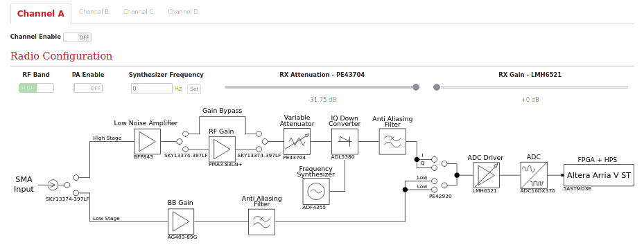
1.1. Rx Web UI Controls
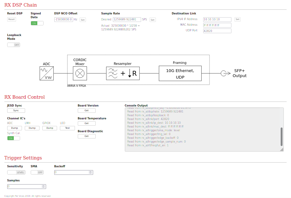
This page, as shown in Figure 1 allows the configuration of the entire receive chain (A-D) from the RF front end to the digital backend. First, you must select the channel that is being configured or monitored. This page allows for radio configuration (gain, attenuation, LO frequency, and band selection), as well as providing Rx DSP controls (NCO Offset, sample rate, and destination ports). Moreover, you can get information about the board (version, temperature, diagnostic) and do testing. Trigger settings can also be configured here.
The basic Rx signal chain is as follows: a signal is first sampled from the antenna which is connected to the SMA connector on the Crimson. The analog signal is fed through an RF switch based on the frequency of the signal being sampled. High band is reserved for signals greater than 500 MHz, and the low band is reserved for signals less than 500 MHz. Crimson currently supports signals up to 6 GHz. Within the respective RF chains (high and low) it filters the analog signal and divides it into I and Q channels for advanced signal processing on the FPGA. The high band offers an LNA for weaker signals, and a frequency mixer for desired intermediate frequencies prior to signal processing. The low band offers a varactor circuit to fine tune the delay between the I and Q channel. An ADC driver is common between both bands (high and low) prior to the ADC. The ADC will send the data across to the DSP chain within the FPGA at a rate of 322 MSPS using the JESD serial interface. The DSP chain will downsample the samples resulting in an adjusted final sample rate. The frequency of the signal can be adjusted prior to decimation. A more thorough description of the Rx signal chain is on the SDR Frequency Tuning Mechanics application note.
Figure 1: Rx Web UI.
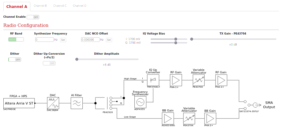
1.2. Tx Web UI Controls
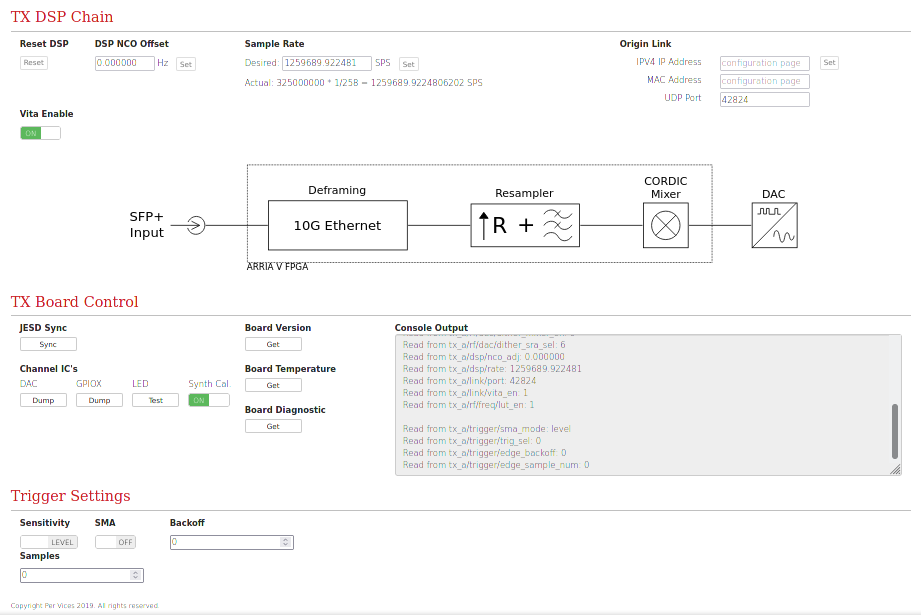
This page, as shown in Figure 2 allows the configuration of the entire transmit chain from the digital backend to the RF frontend. Similar to Rx, you must first select the channel that is being configured. In the radio configuration section, you are able to set various RF parameters (synthesizer frequency, DAC NCO offset, IQ Voltage Bias, dither and gain). In the Tx DSP chains, you are able to configure sample rates and DSP NCO offsets, as well as configure the IP/MAC address links and UDP port. Moreover, you can get information about the board (version, temperature, diagnostic) and do testing. Trigger settings can also be configured here.
The basic Tx signal chain is as follows: first, the digital signal comes from the FPGA and gets interpolated through the DSP chain on the FPGA. The interpolation can go up to a maximum of 322 MSPS and can be frequency adjusted prior to DAC conversion. The digital signal is sent to the RF frontend using the JESD serial interface, providing the DAC with both IQ channel values. The analog signal passes through an RF switch for high band and low band selection. The high band is reserved for signals greater than 500 MHz and the low band is reserved for signals under 500 MHz. The high band offers a frequency mixer for up-conversion up to a maximum of 6 GHz. A more thorough description of the Tx signal chain is on the SDR Frequency Tuning Mechanics application note.
Figure 2: Tx Web UI.
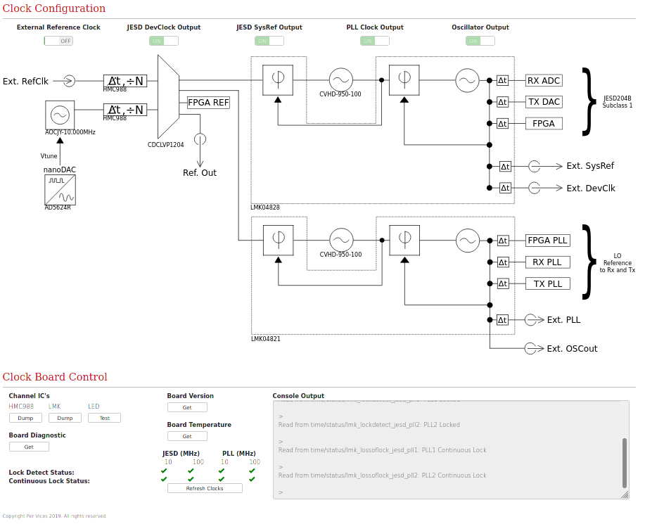
1.3. Clock Web UI Controls
The synth board is used for generating all of the clocks for the Digital, TX, and RX boards. This includes the on board IC clocks, JESD sysref clock, and synthesizer clocks. As shown in Figure 3 below, there are a couple of configurations that are possible with the synth board. The 10MHz clock reference can be chosen between an internal or external SMA source. Moving along to the right side of the chain, the 10MHz steps up to 100MHz with a feedback circuit. This architecture maintains the high 10MHz source precision with low phase noise associated with the 100MHz PLL. The fanout buffer will propagate the 100MHz signal to the other boards (RX, TX, and Digital), and feed the LMK04828 to generate the JESD compliant signals. In addition, you are able to choose which clocks are on and off by the toggle in the web UI.
Figure 3: Clock Web UI.
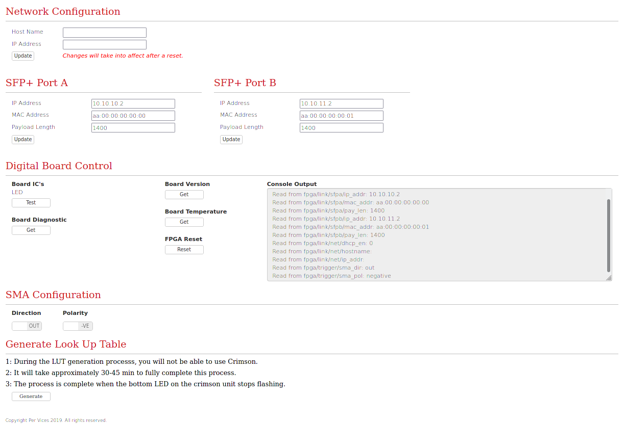
1.4. Configuration Web UI
This Web UI page, as shown in Figure 4 below, allows for configuration of the network, and SFP ports. Moreover, it allows you to retrieve information and test the digital board. Configuration of the SMA for direction and polarity is also possible here.
The digital board houses the FPGA with the SoC ARM Cortex-A9 Processor and hard processing system for JESD communication between the boards. The digital board is required for communicating with the RX and TX board, and retrieves all of the clocks through the Synth board. The digital board supports 20Gbps using dual 10GbE and digital down/up conversion on the FPGA with Per Vices DSP IP core. The ADC and DAC chains that you see refer to the hardware running on the Arria V ST FPGA. It includes a series of filters before it feeds to and from the 10GbE SFP + Port (i.e. SFP+ A and SFP+ B).
Figure 4: Configuration Web UI.
2. Cyan Web UI
Note
This is still under development. More information will be posted soon.